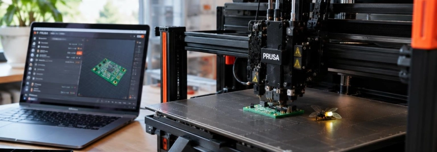
A desktop 3D printer can pick up a resistor, place it inside a part being manufactured, and leave an electronic device ready to work when printing is finished. That is the principle behind Print & Place, a system created by researchers at the University of Bristol and the Hasso Plattner Institute that makes use of ordinary FDM printers without modifying their hardware.
The technique turns the print head into a pick-and-place tool. Instead of adding a dedicated mechanism, it deposits a small amount of filament onto the component, waits for it to cool and adhere, then transports it to the intended point on the object. The component is then released by reheating the filament to its melting point or by using a rapid movement of the print head to cut it through shear.
The approach aims to manufacture functional electronic devices by integrating component placement, electrical connections, and encapsulation into the printing process itself. The team also presented a workflow for preparing the job and generating a tray for loading the components.
“Print & Place is a novel process that appropriates unmodified commodity FDM 3D printers to enable in-situ pick-and-place of electronic components”
— the researchers
Filament as an assembly tool
The method relies on the adhesion of a drop of extruded, cooled thermoplastic. The print head uses it to pick up a component and place it on the appropriate layer of the structure being built. When it is time to release it, the filament can be melted again or broken by a sudden movement of the tool.
The work covers everything from individual components and conductive traces to assembled printed circuit boards. The printer alternates between building the structure and placing these parts; as printing continues, it can leave them connected and enclosed within the object. This means the electronics do not necessarily have to be added by hand after removing the part from the build plate.
The Hasso Plattner Institute describes a workflow that combines mechanical and electronic design with job preparation. Users design the object and its circuits in a Rhino plugin, which also generates the component tray. They then load the parts into this printed tray, and the machine picks them up and places them on the specified layer.
Hackster.io explains that the custom software handles both printing the temporary component tray and executing the placement movements. The printer does not need to be modified, although the process does involve designing the object, preparing the parts, and using a program that coordinates printing with assembly.
A Prusa XL, 0805 parts, and a 0603 barrier
The prototype was built around an unmodified Prusa XL. The team chose it for its large print area, which leaves room for the component tray alongside the model. For the tests, they used PLA filament from Bambu Lab and Elegoo.
The machine was able to pick up and place surface-mount components as small as size 0805, as well as conductive traces as thin as 1.25 mm. It also worked with printed circuit boards up to the size of an Adafruit Flora development board.
The test had a clear limit: a 0603 resistor proved too small for the system. This result defines the minimum size the prototype could handle; the published figures do not describe a universal capability for any printer or component, but rather the tests carried out by the team with its setup.
The choice of an unmodified printer is central to the proposal: the system reuses the print head and filament of an available FDM machine, rather than requiring a platform designed from scratch to assemble circuits. However, the method depends on being able to pick up, transport, and release the part reliably; the 0603 resistor was the specific example that fell outside the demonstrated capabilities.
From a glowing caterpillar to a robot that walks off the build plate
The devices manufactured include an illuminated articulated caterpillar, an LED refrigerator magnet, and a robotic firefly that moves by vibrating. The demonstrations show that Print & Place is not limited to depositing components inside a housing: it integrates electronic parts into objects that can perform a function.
The firefly is the most striking example of the complete workflow. The team designed it to be ready to work as soon as printing was finished and to “walk” off the build plate on its own. The Hasso Plattner Institute also highlights a small robot capable of walking off the base once complete, and shows an illuminated magnet among the other objects manufactured.
The goal is to avoid some of the steps that typically separate printing an object from using it: manually assembling components, extensive post-processing, or resorting to filaments with high electrical resistance. The researchers argue that automating placement, electrical connection, and encapsulation during manufacturing expands the range of devices that can be produced through additive manufacturing.
This does not mean that every electronic design can simply be transferred to the printer. The reported tests have size limitations, and the demonstration relies on a workflow prepared to design the part and generate the placement movements. The team does show a way to manufacture assemblies that include discrete components, traces, and boards, within the capabilities of the tested system.
Publication and a conflicting bibliographic reference
Hackster.io reports that the work was published in the proceedings of the 39th ACM Symposium on User Interface Software and Technology, UIST ’26, with open access. The Hasso Plattner Institute page, by contrast, lists the publication as “Print & Place” in the proceedings of CHI’26 and also includes the mention “UIST 2026 BEST PAPER AWARD”. The two pages therefore do not agree on how they identify the proceedings associated with the work.
The Hasso Plattner Institute credits Oliver Child, Patrick Baudisch, and Mike Fraser with the project. The page places it within the Human Computer Interaction Lab, whose stated goal is to bring the computer’s virtual world and the user’s physical world together in the same space.
The published demonstration provides a practical reference in the form of the specific setup tested: an intact Prusa XL, PLA from Bambu Lab and Elegoo, 0805 components as the smallest size demonstrated, and a board the size of an Adafruit Flora as the largest described. The 0603 resistor, too small in these tests, marks the most precise limit reported by the team.
Sources: Hackster.io, Hasso Plattner Institute